

MTIP has high electron mobility, making it a good candidate for future electronic device applications. Furthermore, MTIP has good transport properties and chemical interactions in non-polar solvents such as chloroform, dichloromethane, and acetonitrile. The phase transition temperature is also relatively low, about 70°C, and the crystal structure is still stable below 400°C. The optical properties of MTIP depend on the orientation of the crystallographic planes relative to incident light.
| Purity | 99% |
| Appearance | black solid |
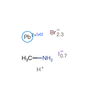
| Linear Formula | CH6I3NPb |
| CAS Number | 69507-98-8 |
| Mol. Weiga | 919.98 |
| Stock Name | MAPbI3 |
| Name(EN) | MAPbI3 |
| Synonym | CH3NH3PbI3/MAPbI3 |
Heterogeneous semiconductor nanowire array for sensitive broadband photodetector by crack photolithography-based micro-/nanofluidic platforms
Introduction Semiconductor nanowires (NWs) are widely used for electronics,1 bio/chemical sensors,2 lasers,3 and photodetectors4–7 for their uniquely high surface-to-volume ratio that enables high sensitivity, rapid response time, and low power consumption.8 However, their fabrication methods typically rely on traditional micro-/nanofabrication equipment and facilities so precisely controlling the number, dimensions, orientation, alignment, and position of NWs on the same substrate9 remains a challenge. For example, chemical vapor deposition (CVD) has the general advantage of precise surface, morphology, structure, and composition control of a product, thus providing an alternative synthesis route toward high quality single-crystalline semiconductor nanowires.10,11 However it is difficult to directly use the nanowires prepared by CVD methods in the devices based on a single nanowire without manipulation and transfer. The integration of NWs into the nano-/microelectromechanical
The in situ growth of nanowires (NWs) into nano-/microelectromechanical systems (NEMS/MEMS) by solution processing is attractive for its relative simplicity and economic value. We present innovative, versatile microfabrication that produces multiple, heterogeneous semiconductor NWs. A crack photolithography-based micro-/nanofluidic platform has been developed. This platform offers the in situ solution growth of NWs while enabling the control of quantity, dimensions, orientation, alignment, position, and material. The generation of grain boundary (GB)-rich CH3NH3PbI3 NWs using the micro-/nanofluidic device is exemplary. High-quality single-crystal CH3NH3PbI3 NWs were derived by injection of a CH3NH3PbI3 solution. We produced a parallel NW array of CH3NH3PbI3 NW for visible light detection and ZnO NW for ultraviolet detection, thereby demonstrating an unprecedented broadband composite photodetector. The micro-/nanofluidic fabrication platform enables the production of multiple, heterogeneous semiconductor NW arrays on one substrate, offering the potential to elicit synergistic performance and functional enhancements from various NWs.
Effect of the heat treatment of CH3NH3PbI3 perovskite on its electrical and photoelectric properties
Amasev, Dmitriy V.; Kazanskii, Andrey G.; Mikhalevich, Vladislav G.; Saitov, Shamil R.; Tameev, Alexey R. [Mendeleev Communications, 2021, vol. 31, # 4, p. 469 - 470]
Abstract
| Characteristic 1 | I |
| Characteristic 2 | Pb |